

 How to resolve AdBlock issue?
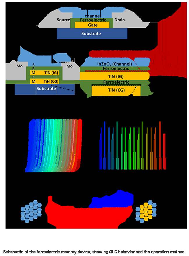
In an era characterized by an exponential surge in data production and processing, researchers at Pohang University of Science and Technology (POSTECH) in South Korea have achieved a significant breakthrough in memory technology. Against the backdrop of escalating demands for efficient and high-capacity data storage, their groundbreaking advancements in hafnia-based ferroelectric memory devices hold remarkable promise for the future of data storage.
Led by Professor Jang-Sik Lee from the Departments of Materials Science and Engineering and Semiconductor Engineering, the research team at POSTECH has revolutionized the field of memory technology by dramatically increasing the data storage capacity of ferroelectric memory devices. By combining hafnia-based materials with an innovative device structure, their groundbreaking findings have placed memory technology on an evolutionary trajectory.
The ever-increasing amount of data generated due to advancements in electronics and artificial intelligence (AI) has necessitated a corresponding leap forward in data storage technologies. While NAND flash memory has served as a widely used technology for mass data storage, its reliance on charge traps for data storage leads to higher operating voltages and slower speeds. Recognizing this bottleneck, the research team at POSTECH turned to hafnia-based ferroelectric memory as a compelling alternative.
At the core of their research lies hafnia (Hafnium oxide), a material that enables ferroelectric memories to operate at low voltages and high speeds. However, until now, the limited memory window for multilevel data storage has presented a significant challenge. The team at POSTECH, under the guidance of Professor Jang-Sik Lee, effectively addressed this limitation by introducing new materials and an innovative device structure.
By introducing aluminum-doped ferroelectric materials, the team elevated the performance of hafnia-based memory devices, demonstrating the potential of high-performance ferroelectric thin films. In addition, they revolutionized the structure of the device itself, shifting from the conventional metal-ferroelectric-semiconductor (MFS) design to a novel metal-ferroelectric-metal-ferroelectric-semiconductor (MFMFS) structure.
The team's breakthrough lies in their ability to control the voltage across each layer through carefully fine-tuning factors such as the thickness and area ratio of the metal-to-metal and metal-to-channel ferroelectric layers. This efficient utilization of applied voltage significantly enhances performance while reducing energy consumption.
Conventional hafnia-based ferroelectric devices typically possess a memory window of approximately 2 volts (V). Remarkably, the team at POSTECH surpassed this limitation by achieving a memory window exceeding 10 V, facilitating the implementation of Quad-Level Cell (QLC) technology. With QLC, the research team's memory device can store 16 levels of data (4 bits) per unit transistor, enhancing data storage density.
The team's memory device displayed exceptional stability, remaining steadfast after one million cycles, and operated at voltages of 10V or less. Notably, this is significantly lower than the 18V required for NAND flash memory. The device also exhibited consistent data retention characteristics, ensuring the reliability of long-term data storage.
In contrast to the Incremental Step Pulse Programming (ISPP) method employed by NAND flash memory, the team's device achieves rapid programming through one-shot programming by controlling ferroelectric polarization switching. This breakthrough promises not only faster programming times but also the potential for simplified circuitry.
Expressing his enthusiasm, Professor Jang-Sik Lee of POSTECH stated, "We have laid the technological foundation for overcoming the limitations of existing memory devices and provided a new research direction for hafnia-based ferroelectric memory." He further emphasized his commitment to conducting follow-up research, aiming to develop low-power, high-speed, and high-density memory devices. Such advancements hold the potential to address power issues prevalent in data centers and artificial intelligence applications.
The research conducted by Professor Jang-Sik Lee's team at POSTECH has received support from the Project for Next-generation Intelligent Semiconductor Technology Development, sponsored by the Ministry of Science and ICT (National Research Foundation of Korea) and Samsung Electronics.
As the researchers forge ahead, diverse perspectives come to the forefront, driven by the possibilities presented by this breakthrough. From a scientific standpoint, the achievement offers a glimmer of hope for transforming data storage capabilities, enabling a new era of information processing. However, it is vital to consider the meticulous validation and thoughtful examination of developed technologies to ensure ethical and secure implementation.
With further research and collaboration, the groundbreaking advancements in memory technology by the POSTECH research team hold immense promise. As the demand for data storage solutions grows exponentially, the successful integration of hafnia-based ferroelectric memory devices has the potential to revolutionize the landscape of memory technology, transcending existing limitations and further propelling the digital revolution forward.