

New claim: semiconductor turns superconductor
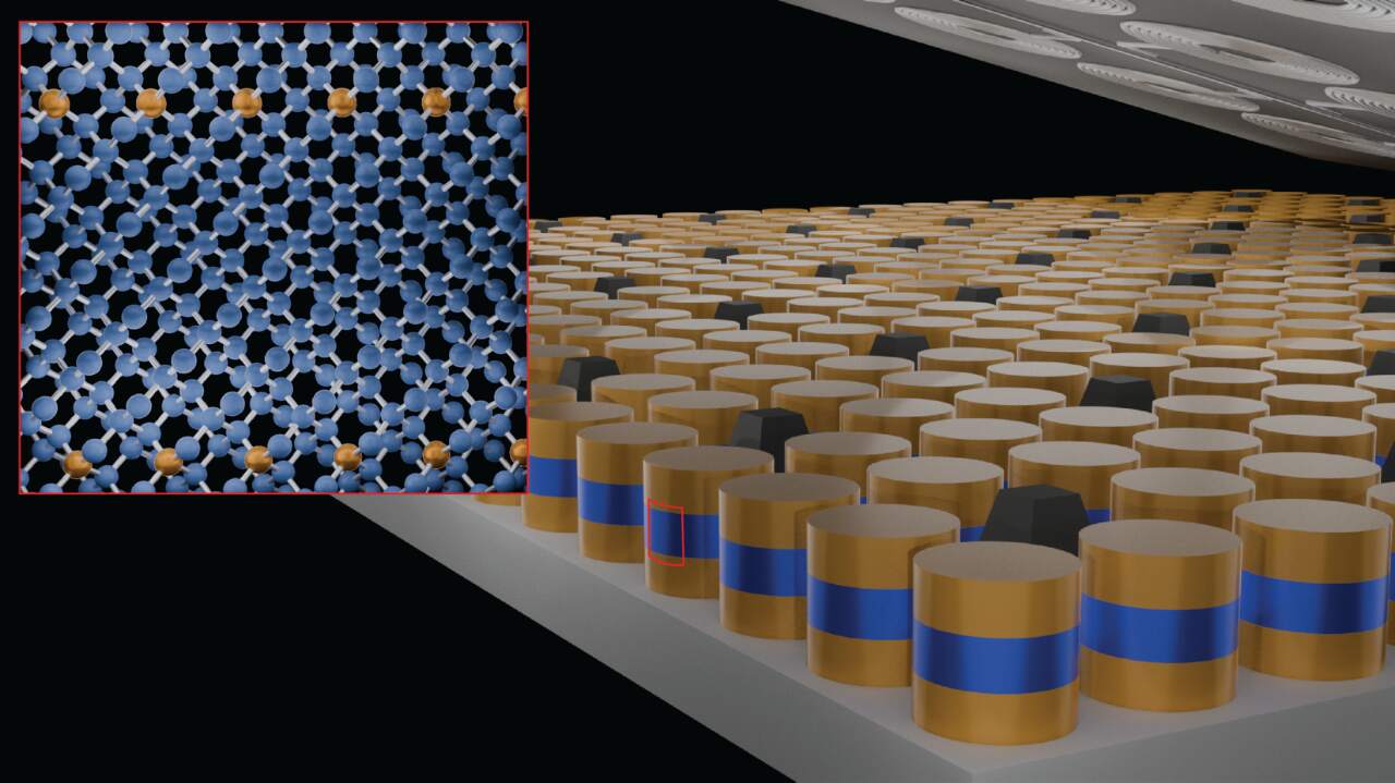
Researchers at New York University (NYU), in collaboration with teams from the University of Queensland, ETH Zürich, and Ohio State University, report the creation of a novel material: hyper-doped germanium (Ge) with gallium (Ga) substitution, which the authors claim exhibits superconductivity at approximately 3.5 K.
According to the published paper in Nature Nanotechnology titled “Superconductivity in substitutional Ga-hyperdoped Ge epitaxial thin films,” the key points are:
- Ga atoms were substitutionally incorporated into the Ge lattice at very high concentrations (~17.9 % Ga substitution, hole concentration ≈ 4.15 × 10²¹ cm⁻³).
- The material was grown epitaxially by molecular-beam epitaxy (MBE), yielding a relatively ordered (low-disorder) structure compared to prior “hyper-doped” attempts.
- The team measured a superconducting critical temperature (T_c) of 3.5 K.
- The authors suggest that this development could serve as a “superconductor–semiconductor platform” within the familiar group-IV semiconductor environment.
NYU’s press materials frame the work as a step toward “scalable, foundry-ready quantum devices”, “low-power cryogenic electronics,” and the integration of classical and quantum chips.
From the vantage of high-performance computing (HPC) and supercomputing infrastructure, the implications of a semiconductor material that also superconducts are enticing:
- If one could integrate superconducting circuits with semiconducting chip infrastructure, one might reduce resistive energy losses, perhaps enabling faster interconnects, denser cryogenic processors, or more efficient quantum-accelerated hardware.
- The fact that the base material is germanium (Ge), which already features in advanced semiconductor processes, prompts optimism about compatibility with existing fabrication pipelines and with chip-scale superconducting/semiconducting hybrids.
- Lower energy dissipation is especially significant for supercomputing centers, where power and cooling are major cost/constraint factors.
However, and importantly, the paper and associated press material also reveal significant limitations, which a skeptical observer must highlight:
- A very low operating temperature of 3.5 K presents a significant challenge. While superconducting quantum circuits can function at millikelvin or low kelvin temperatures, the need for cryogenics remains demanding. For conventional supercomputing hardware, which typically operates at around 300 K or even with moderate cryogenic cooling, the practical application of this technology is uncertain.
- Thin-film, experimental material: The reported material is an epitaxial thin film grown under highly controlled conditions (MBE) with extreme doping levels and careful crystallographic ordering. Scaling this to large-area wafers, reliable yields, multilayer integration, packaging, and thermal/cryogenic infrastructure is non-trivial.
- Limited performance metrics beyond superconductivity: The paper reports the existence of superconductivity, but does not (at least in the abstract) provide data on other performance metrics relevant to supercomputing: e.g., critical current densities, magnetic-field resilience, junction behaviour, switching speeds, coherence/phase noise, integration with semiconducting logic, thermal cycling, and long-term reliability.
- Integration and interface issues: The promise of “superconductor–semiconductor platform” hinges on clean interfaces and controlled doping, but real supercomputing systems require complex multilayer interconnects, packaging, and rugged environments. Translating lab-scale thin films into full system components is a long road.
- Scope inflation risk: The press releases use terms like "scalable," "foundry-ready," and "quantum devices and low-power cryogenic electronics," which seem to overstate the current findings. There's a clear gap between demonstrating superconductivity in a thin film and deploying it in actual supercomputing hardware.
To be clear: this work does not yet change the supercomputing landscape. Among the missing pieces:
- No demonstration of a computing circuit or interconnect built from this material running at supercomputing speeds or under realistic loads.
- No evidence of a full logic device or even a prototype cryogenic classical logic device using the new material.
- No cost/footprint or manufacturing path analysis. The material may require exotic fabrication, extreme cooling, or doping regimes impractical for commercial processors or HPC centers.
- No benchmark against existing superconducting interconnects (e.g., Nb, NbTi, high-Tc materials) or advanced semiconductor interconnects.
- No demonstration of switching speeds, control logic, or system scalability.
In other words, the headline “semiconductor that superconducts” is accurate, but the leap to “supercomputing revolution” is not yet justified.
Why this still matters, cautiously
Despite the caveats, this research is interesting and worth tracking for these reasons:
- It demonstrates that superconductivity can be achieved in a group-IV semiconductor environment (germanium) with relatively low disorder, opening a novel materials platform.
- It could enable new hybrid architectures where semiconducting and superconducting components are integrated more closely on a chip, potentially reducing interconnect parasitics and thermal mismatches.
- For cryogenic computing architectures (emerging research field: cryo-cooled classical logic, deep-learning at low temperatures, superconducting logic), having a more “familiar” semiconductor substrate might reduce integration complexity compared to exotic superconductors alone.
- From a materials science standpoint, identifying substitutional Ga in Ge, along with the resulting structural distortion (tetragonal distortion) and high hole concentration, significantly contributes to our understanding of superconductivity in non-metallic materials.
Outlook and key questions for supercomputers
Here are questions supercomputing architects and technology watchers should ask when evaluating this kind of research for future applicability:
- What is the critical current density (Jₙ) of this Ge:Ga superconductor, and how does it compare to existing superconductors used for interconnects or logic?
- How robust is the superconductivity under magnetic fields, temperature cycling, thermal load, and mechanical stress? HPC environments impose non-ideal conditions.
- Can this material be fabricated at the wafer scale, with high yield, multi-layer connectivity, and compatible with high-volume semiconductor fabrication?
- Can circuits be built that take advantage of the superconductivity (e.g., superconducting interconnects, logic, sensors) and integrate with classical CMOS/Ge logic in the same chip or module?
- What is the energy/cost trade-off when including the required cryogenic cooling, packaging, and supporting infrastructure? Does the reduction in resistive loss offset the additional overhead in cooling and system complexity?
- Do the superconducting transition and operation domain align with the operating conditions of a practical supercomputer module (i.e., cooling budget, maintenance, reliability)?
- Are there unanticipated material limitations, e.g., dopant clustering over time, degradation, interface mismatches, or manufacturing variability that would hamper mass deployment?
In summary, the announcement from NYU and collaborators represents a noteworthy advance in materials science; the creation of a superconducting thin film from germanium is a significant achievement. However, for the supercomputing field, it is premature to characterize this as a breakthrough that will reshape HPC architectures. Demonstrations of fabrication scale-up, device performance, system integration, cost-effectiveness, and reliability are still needed.
Until those pieces fall into place, the hype surrounding "scalable quantum devices" or "foundry-ready superconducting semiconductors" should be tempered with caution. The future may indeed bring hybrid semiconductor-superconductor chips, low-power cryogenic logic, and novel interconnects, but this research represents a significant step, not the final destination.