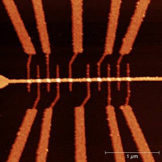
Scientists from the University of Twente’s MESA+ research institute have developed a method for studying individual defects in transistors. All computer chips, which are each made up of huge numbers of transistors, contain millions of minor ‘flaws’. Previously it was only possible to study these flaws in large numbers. However, fundamental research conducted by University of Twente scientists has now made it possible to zoom in on defects and study them individually. In due course, this knowledge will be highly relevant to the further development of the semiconductor industry. The research results were published today in Scientific Reports, a leading scientific journal produced by the Nature Publishing Group.
Computer chips typically contain numerous extremely small defects. There are often as many as ten billion defects per square centimetre. The bulk of these defects cause no problems in practice, but the large numbers involved pose enormous challenges for the industry. This is just one of the barriers to the further miniaturization of chips, based on existing technology. It is, therefore, vital to obtain a detailed understanding of how these defects arise, of where they are located, and of how they behave. Until now it has been impossible to study individual defects, due to the large number of defects on each chip, and the fact that closely spaced defects influence each other. For this reason, the defects were always studied in ensembles of several million at a time. However, this approach suffers from the drawback that it only yields a limited amount of information on individual defects.
Main tap
A group of University of Twente researchers led by Dr Floris Zwanenburg have now developed a clever method that, at long last, makes it possible to study individual defects in transistors. Working in the University of Twente’s NanoLab, the researchers first created chips containing eleven electrodes. These consisted of a group of ten electrodes 35 nanometres wide and, located perpendicularly above them, a single electrode 80 nanometres long (a nanometre is one million times smaller than a millimetre). Dr Zwanenburg compares these electrodes to taps – not for water, but for electrons – which the researchers can turn on and off. The researchers first turn on the long electrode, the ‘stopcock’. At a temperature of -270 degrees Celsius, they then open or close the other ‘taps’. This enables them to locate the ‘leaks’, or – in other words – identify the electrodes beneath which defects are located. It turned out that there were leaks under every single electrode.
Neutralizing the defects
In a subsequent step, the researchers were able to neutralize more than eighty percent of the defects by heating the chips to 300 degrees Celsius, in a furnace filled with argon. In some cases, there was only a single defect beneath a given electrode. Having reduced the density of defects in the material, the researchers were then able to study individual defects. Floris Zwanenburg explains that “The behaviour of individual defects is of great importance, as it will improve our understanding of defects in contemporary electronics. Of course, the electronics in question work at room temperature and not at the extremely low temperatures used in our study. Nevertheless, this is an important step for fundamental research and, ultimately, for the further development of modern IC technology.”
Research
The research was conducted by Paul-Christiaan Spruijtenburg, Sergey Amitonov, Filipp Mueller, Wilfred van der Wiel and Floris Zwanenburg of the Department of NanoElectronics, at the University of Twente’s MESA+ Institute for Nanotechnology. The study was jointly funded by the European Commission and the FOM Foundation. 


 How to resolve AdBlock issue?