GOVERNMENT
Future sparkles for diamond-based quantum technology
Two research breakthroughs are poised to accelerate the development of synthetic diamond-based quantum technology
Marilyn Monroe famously sang that diamonds are a girl's best friend, but they are also very popular with quantum scientists - with two new research breakthroughs poised to accelerate the development of synthetic diamond-based quantum technology, improve scalability, and dramatically reduce manufacturing costs.
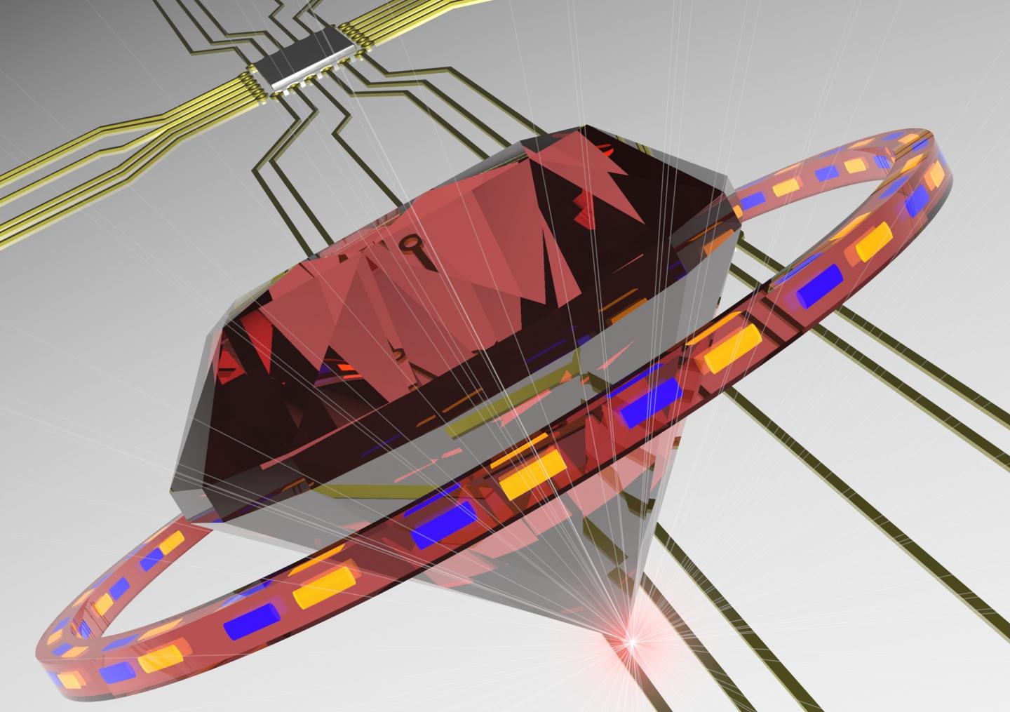
While silicon is traditionally used for computer and mobile phone hardware, diamond has unique properties that make it particularly useful as a base for emerging quantum technologies such as quantum supercomputers, secure communications, and sensors.
However, there are two key problems; cost, and difficulty in fabricating the single-crystal diamond layer, which is smaller than one-millionth of a meter.
A research team from the ARC Centre of Excellence for Transformative Meta-Optics at the University of Technology Sydney (UTS) led by Professor Igor Aharonovich has just published two research papers Nanoscale and Advanced Quantum Technologies, that address these challenges. 
"For a diamond to be used in quantum applications, we need to precise engineer 'optical defects' in the diamond devices - cavities and waveguides - to control, manipulate and read out information in the form of qubits - the quantum version of classical computer bits," said Professor Aharonovich.
"It's akin to cutting holes or carving gullies in a super-thin sheet of diamond, to ensure light travels and bounces in the desired direction," he said.
To overcome the "etching" challenge, the researchers developed a new hard masking method, which uses a thin metallic tungsten layer to pattern the diamond nanostructure, enabling the creation of one-dimensional photonic crystal cavities.
"The use of tungsten as a hard mask addresses several drawbacks of diamond fabrication. It acts as a uniform restraining conductive layer to improve the viability of electron beam lithography at nanoscale resolution," said the lead author of a paper in Nanoscale, UTS Ph.D. candidate Blake Regan.
"It also allows the post-fabrication transfer of diamond devices onto the substrate of choice under ambient conditions. And the process can be further automated, to create modular components for diamond-based quantum photonic circuitry," he said.
The tungsten layer is 30nm wide - around 10,000 times thinner than a human hair - however, it enabled a diamond to etch of over 300nm, a record selectivity for diamond processing.
A further advantage is that removal of the tungsten mask does not require the use of hydrofluoric acid - one of the most dangerous acids currently in use - so this also significantly improves the safety and accessibility of the diamond nanofabrication process.
To address cost and improve scalability, the team further developed an innovative step to grow single-crystal diamond photonic structures with embedded quantum defects from a polycrystalline substrate.
"Our process relies on a lower-cost large polycrystalline diamond, which is available as large wafers, unlike the traditionally used high-quality single crystal diamond, which is limited to a few mm2," said UTS Ph.D. candidate Milad Nonahal, lead author of the study in Advanced Quantum Technologies.
"To the best of our knowledge, we offer the first evidence of the growth of a single crystal diamond structure from a polycrystalline material using a bottom-up approach - like growing flowers from seed," he added.
"Our method eliminates the need for expensive diamond materials and the use of ion implantation, which is key to accelerating the commercialization of diamond quantum hardware," said UTS Dr. Mehran Kianinia, a senior author on the second study.
