US consumers lost $3.49 billion in 2021 YTD to various types of internet crime, $1.58 billion more than damages in 2020

The wave of cybercrime is plowing throughout America with the biggest damages in history.

Atlas VPN extracted data from publicly available government sources and found that US citizens already lost $3.49 billion to cybercrime in the first three quarters of 2021. You don’t need to bring out the calculator - the damages come out to $12.78 million per day.

Edward Garb, a cybersecurity researcher at Atlas VPN explains the main driving forces behind the surge in cybercrime damages: “Cybercriminals are using the buzz around cryptocurrencies, NFTs, and the metaverse to trick people into investing in bogus projects that disappear after raising a hefty sum of money.” vcsprasset 3737091 119386 2e8f 1 0c6fd

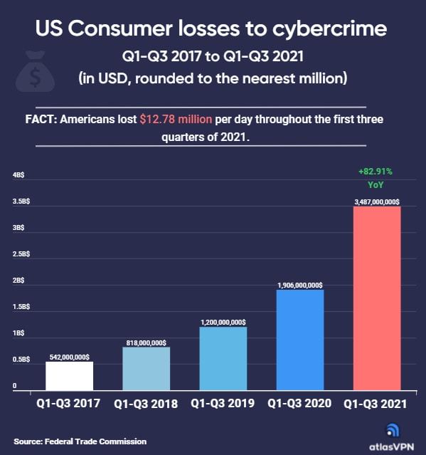
The data for the analysis is based on reports submitted through the official Federal Trade Commission websites -  IdentityTheft.gov and ReportFraud.ftc.gov. Citizens can get help by receiving personal identity theft recovery plans. Regarding monetary damages - the FTC does not resolve the allegations, but it does disseminate the information to over 3,000 law enforcement agencies across the United States for further investigation.

The analysis reveals that cybercrime damages sky-rocketed by 82.91% in 2021 compared to last year. To be exact, people lost $1.58 billion more (yes, billion) this year than they did in the same period in 2020.

These losses are a result of 1.6 million unique fraud and identity theft reports submitted to the Federal Trade Commission websites mentioned previously.  This means that the FTC has to deal with around 5,869 complaints every single day.

Last year, the number of reports stood at 1.09 million after the first three quarters of the year, which is around a third less than in 2021. Back then, they had to go through 3,981 complaints daily.

Most damaging types of cybercrime

To better understand the current cybercrime landscape, we will analyze which crimes caused the most trouble.

We already noted that investment-related crimes are on the rise due to countless projects in the crypto, NFT, and metaverse markets. This year, US citizens lost a staggering $956 million to these types of scams, representing a 277.87% growth YoY.

To read the full paper, head over to:

https://atlasvpn.com/blog/americans-lost-a-record-3-5bn-to-cybercrime-in-2021-ytd
 

China introduces an all-optical supercomputing chip scheme based on CNNs

In a new publication from Opto-Electronic AdvancesDOI10.29026/oea.2021.200060, the research group of Professor Xiaoyong Hu and Professor Qihuang Gong from School of Physics, Peking University, China, propose a new strategy to realize an ultrafast and ultralow-energy-consumption all-optical supercomputing chip scheme based on convolutional neural network (CNN), which supports the execution of multiple computing tasks. All-optical transcendental equation solver. (A) schematic diagram of the all-optical transcendental equation solver. (B) Top-view SEM image of the all-optical transcendental equation solver, where the scale bar is 100 μm. Here, the white dotted lines mark the five layers for waveform discretization, and the red dotted lines separate the three layers of the optical CNN structure. (C) Output light intensity distribution in the output waveguides (k = 1.67). The arrows in the figure correspond to the locations of the solutions. The horizontal axis is the number of discrete waveguides, the vertical axis on the right represents the output signal intensity, and the vertical axis on the left gives the deviation between the experimental output signal and the theoretical value. (D) A graphic representation of solution deviation. The horizontal axis labels the individual solutions, and the vertical axis represents three values of the parameter k. The shade of the color indicates the magnitude of the deviation. Full size

With the rapid development of advanced engineering computing, economic data analysis, and cloud computing, the demand for ultra-high-speed and energy-efficiency supercomputing is growing exponentially. Due to the limited data communication bandwidth between memory and processor, the inherent RC delay of the integrated circuit, and the heat dissipation caused by resistance loss in the electronic circuit, the dominant computing platform, namely the traditional electronic signal processor under von Neumann architecture is difficult to achieve high speed and low energy consumption at the same time.

All-optical computing using photons as an information carrier provides a potential alternative to the traditional electronic signal processor. However, there is an inherent trade-off that the larger nonlinear coefficient can only be at the expense of the slower response time. This trade-off poses a major challenge to the construction of integrated photonic processors based on von Neumann architecture, which usually requires complex heterogeneous integration of various photonic devices in a single chip. Therefore, it is urgent to explore new architecture and unconventional all-optical supercomputing schemes.

The research group of Prof. Xiaoyong Hu and Prof. Qihuang Gong from the School of Physics, Peking University, proposes a new strategy to realize an ultrafast and ultralow-energy-consumption all-optical computing chip scheme based on a convolutional neural network (CNN), which supports the execution of multiple computing tasks. The optical CNN consists of cascaded silicon Y-shaped waveguides with side-coupled silicon waveguide segments designed to control the amplitude and phase of light in the waveguide branches. As a proof-of-concept, they experimentally implemented the network design through several computation tasks including transcendental equations solvers, multifunctional logic gate operators, and half-adders. The time-of-flight of light through the network structure corresponds to an ultrafast computing time of the order of several picoseconds with an ultralow energy consumption of dozens of femtojoules per bit. Their approach can be further expanded to offer the possibility of parallel computing using wavelength multiplexing based on non-von Neumann architectures and thus paves a new way for on-chip all-optical computing.
cos2kx+4=tan(kx)

For example, a transcendental equation solver has been achieved to solve the above equation with high accuracy with a maximum deviation of less than 5%, and in most cases, the deviations are less than 3%. The accuracy of the solution can be improved by increasing the number of output waveguides in theory. Besides excellent solution accuracy, the all-optical equation solver also features ultrafast (The time-of-flight of light passing through the characteristic structure is ~1.3 ps) and energy-efficiency computation (~92 fJ/bit ). Stability analysis of their network further demonstrates its high fault tolerance to defects such as weight deviation and waveguide damage. This work, therefore, points to a promising direction for next-generation all-optical computing systems.

Stuttgart researchers work on integrating color centers into nanophotonic silicon carbide structures

Research into superfast quantum computers is now well advanced, but it is not yet possible to connect the individual processors. An international research team with participation from the University of Stuttgart in Germany has now shown a way to scale quantum supercomputers using nanophotonic silicon carbide structures to solve the problems. 

A promising route towards larger quantum computers is to orchestrate multiple task-optimized smaller systems. To dynamically connect and entangle any two systems, photonic interference emerges as a powerful method, due to its compatibility with on-chip devices and long-distance propagation in quantum networks.

One of the main obstacles towards the commercialization of quantum photonics remains the nanoscale fabrication and integration of scalable quantum systems due to their notorious sensitivity to the smallest disturbances in the close environment. This has made it an extraordinary challenge to develop systems that can be used for quantum supercomputing while simultaneously offering an efficient optical interface. Visualization of a VSi center integrated into a nanophotonic SiC waveguide. Photo: University of Stuttgart / PI 3

A recent result shows how the integration obstacle can be overcome. The work is based on a multi-national collaboration with researchers from the Universities of Stuttgart in Germany (Physics 3), California - Davis, Linköping, and Kyoto, as well as the Fraunhofer Institute at Erlangen, the Helmholtz Centre at Dresden, and the Leibniz-Institute at Leipzig.

The researchers followed a two-step approach. First, their quantum system of choice is the so-called silicon-vacancy center in silicon carbide, which is known to possess particularly robust spin-optical properties. Second, they fabricated nanophotonic waveguides around these color centers using gentle processing methods that keep the host material essentially free of damage.

“With our approach, we could demonstrate that the excellent spin-optical properties of our color centers are maintained after nanophotonic integration,” says Florian Kaiser, Assistant Professor at the University of Stuttgart, the supervisor of this project. “Thanks to the robustness of our quantum devices, we gained enough headroom to perform quantum gates on multiple nuclear spin qubits. As these spins show very long coherence times, they are excellent for implementing small quantum computers.”

“In this project, we explored the peculiar triangular shape of photonic devices. While this geometry is of commercial appeal because it provides the versatility needed for scalable production, little has been known about its utility for high-performing quantum hardware. Our studies reveal that light emitted by the color center, which carries quantum information across the chip, can be efficiently propagated through a single optical mode. This is a key conclusion for the viability of integration of color centers with other photonic devices, such as nanocavities, optical fiber, and single-photon detectors, needed to realize full functionalities of quantum networking and computing.” – says Marina Radulaski, Assistant Professor at the University of California – Davis.

What makes the silicon carbide platform particularly interesting are its CMOS compatibility and its heavy usage as a high-power semiconductor in electric mobility. The researchers now want to benefit from these aspects to leverage the scalable production of spin-photonics chips. Additionally, they want to implement semiconductor circuitry to electrically initialize and read out the quantum states of their spin qubits. “Maximising electrical control – instead of traditional optical control via lasers – is an important step towards system simplification. The combination of efficient nanophotonics with electrical control will allow us to reliably integrate more quantum systems on one chip, which will result in significant performance gains.”, adds Florian Kaiser, “In this sense, we are only at the dawn of quantum technologies with color centers in silicon carbide. Our successful nanophotonic integration is not only an exciting enabler for distributed quantum computing, but it can also boost the performance of compact quantum sensors.”